Samsung Semiconductor
Founded Year
1974About Samsung Semiconductor
Samsung Semiconductor offers semiconductor technology and operates within the semiconductor industry. It offers products including Dynamic Random Access Memory (DRAM), solid-state drive (SSD), processors, image sensors, and display ICs, which are components for electronic devices. It serves sectors such as mobile, automotive, computer, network, television, gaming, 5G, and Artificial Intelligence (AI) industries. It was founded in 1974 and is based in San Jose, California.
Loading...
ESPs containing Samsung Semiconductor
The ESP matrix leverages data and analyst insight to identify and rank leading companies in a given technology landscape.
The compute-in-memory (CIM) market (also called processor-in-memor, in-compute memory, or computational memory) combines data storage and computational processing within the same memory unit. Instead of the traditional model where data is transferred between separate processing and storage units, CIM performs computations where the data is stored. These solutions significantly reduce data movement…
Samsung Semiconductor named as Outperformer among 15 other companies, including IBM, Cerebras, and SK hynix.
Loading...
Research containing Samsung Semiconductor
Get data-driven expert analysis from the CB Insights Intelligence Unit.
CB Insights Intelligence Analysts have mentioned Samsung Semiconductor in 1 CB Insights research brief, most recently on Sep 13, 2024.
Sep 13, 2024
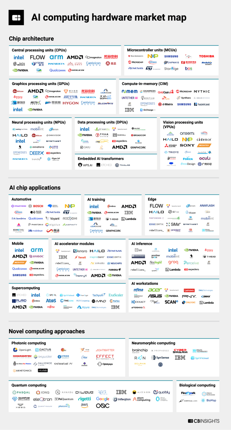
The AI computing hardware market mapExpert Collections containing Samsung Semiconductor
Expert Collections are analyst-curated lists that highlight the companies you need to know in the most important technology spaces.
Samsung Semiconductor is included in 1 Expert Collection, including Semiconductors, Chips, and Advanced Electronics.
Semiconductors, Chips, and Advanced Electronics
7,433 items
Companies in the semiconductors & HPC space, including integrated device manufacturers (IDMs), fabless firms, semiconductor production equipment manufacturers, electronic design automation (EDA), advanced semiconductor material companies, and more
Samsung Semiconductor Patents
Samsung Semiconductor has filed 2 patents.
The 3 most popular patent topics include:
- 3d imaging
- computational complexity theory
- image processing

Application Date | Grant Date | Title | Related Topics | Status |
|---|---|---|---|---|
12/9/2019 | 8/1/2023 | Electromagnetic radiation, Electromagnetism, Optical devices, Waves, Radar | Grant |
Application Date | 12/9/2019 |
|---|---|
Grant Date | 8/1/2023 |
Title | |
Related Topics | Electromagnetic radiation, Electromagnetism, Optical devices, Waves, Radar |
Status | Grant |
Latest Samsung Semiconductor News
Aug 16, 2025
Content Writing Tips: Improve Your Skills & Productivity Joanna Goodrich published: 2025-08-07 18:00:00 Kamal Rudra found the topic of semiconductors pretty boring when he encountered it in high school. But that all changed when he took a college course on semiconductor optoelectronics. The IEEE member credits the class’s professor with sparking his interest in the technology. “His teaching style was engaging and incredibly effective,” Rudra says. “It made me genuinely fall in love with the subject. The combination of hands-on lab experiments and deep theoretical learning finally gave me clarity that this was the field I wanted to pursue.” Kamal Rudra Title: Member grade: Motilal Nehru National Institute of Technology in Allahabad, India; University of Michigan in Ann Arbor A research and development integration engineer at IBM Research in Albany, N.Y., Rudra is now working on back-end-of-line (BEOL) integrated circuits to create copper wiring structures for logic technologies. “With the advent of novel transistor architectures, we are paving the way for faster and more-energy-efficient processors for AI and other uses,” Rudra says. “By improving the BEOL interconnects, RC delay and electromigration can be reduced, ensuring transistor-level gains translate into system-level performance.” The Computer Society recognition “reinforces my belief that I’m moving in the right direction,” Rudra says, “and it encourages me to keep pushing the boundaries of what’s possible in semiconductor technology and computing.” Inspired by a physics teacher Like many engineers, Rudra was fascinated by how things worked as a youngster. Growing up in India, he would take apart remote-controlled cars and use the motors and batteries to build something new. No one in his family worked in science, technology, engineering, or math, he says, but science has always felt “completely natural.” His fascination with STEM subjects deepened in high school, and his teachers fueled his passion. But it was M.R. Shenoy, a physics professor at the Indian Institute of Technology, Delhi , who inspired him to pursue research in the semiconductor field. As an undergraduate at the Motilal Nehru National Institute of Technology , in Allahabad, India, Rudra took an online semiconductor optoelectronics certification course offered by NPTEL that was taught by Shenoy. “These internships were my first real exposure to experimental research and gave me a foundation in device physics and material science,” he says. He earned a bachelor’s degree in electronics and communications engineering from MNNIT in 2019. Working in semiconductor fabrication and FinFET After graduating he became a research assistant at the Indian Institute of Science (IISc), in Bengaluru. There he developed a thin film of manganese vanadium oxide using the epitaxy process. The method grows the manganese vanadium oxide on top of the crystal substrate—which gives engineers more control over the film’s thickness, composition, and crystal structure, according to Photonics Media . Rudra used the film to develop a photodetector for infrared light. After a year he joined semiconductor manufacturer GlobalFoundries , also in Bengaluru, as an integration and yield engineer. He continued his work at IISc on the weekends. “Before joining, I had modest expectations—largely because of the limited semiconductor manufacturing ecosystem in India,” he says. “But I realized that hardware-focused work was indeed happening in the industry. That experience planted the seed of transitioning from academia to cutting-edge industrial R&D.” “For any young professional in STEM, IEEE isn’t just a resource; it’s a launchpad.” While at GlobalFoundries, he worked on BEOL interconnects to enhance the yield of the company’s FinFET chips, which are used in automotive technology, smartphones, and smart speakers. In conventional planar transistors, the gate sits atop a flat silicon channel, controlling the flow of current between the source and drain from only one side. As transistors shrank in size, however, they became less reliable and leaked current, wasting power. FinFET development was led by Chenming Hu , who received the 2020 IEEE Medal of Honor for the invention. FinFET’s 3D structure provides better control of the current. In 2021 Rudra decided to continue his education and was accepted into the master’s degree program in electrical and computer engineering at the University of Michigan in Ann Arbor. “I chose this school because there was a particular professor working on LED devices whose research really resonated with me,” he says. The professor, IEEE Fellow Zetian Mi , was working on III-V semiconductor optoelectronic devices. Rudra was part of Mi’s research team for the first two semesters of his graduate program, working on the fabrication and characterization of III-Nitride-based microLEDs. Rudra also completed an internship at Meta in Redmond, Wash., where he developed integration processes for waveguide-based photonic devices for AR/VR systems. “That experience helped me understand how photonics intersects with semiconductor manufacturing,” he says, “particularly in emerging applications like next-gen displays and wearable optics.” After earning his degree in 2023, he joined Samsung Semiconductor in Austin, Texas, as a device integration engineer. There he returned to working on FinFETs, but this time analyzing and optimizing device and front-end-of-line integration for 14-nm node technology and how different processes affect the electrical performance and yield of FinFETs. After a year, he left to join IBM Research. “Being part of such a high-impact, globally collaborative initiative has been a fantastic experience and one that continues to push me technically and professionally,” he says. Since working at the company, he has filed 22 U.S. patents. He received a slew of honors last year, including being named to Semicon West ’s 20 Under 30 list, the Society of Manufacturing Engineers ’s 30 Under 30, and Semicon Europa ’s 20 Under 30. Recently, he made the Albany Business Review 40 Under 40 list. “These recognitions,” he says, “have been deeply motivating—not just as personal milestones but as validation of the collective work I’ve been part of, and the mentors who’ve helped shape my path.” Making important connections at IEEE Rudra joined IEEE in 2020 after his “Visible Light Response in Defect Engineered Wrinkle Network Nanostructured ZnO” research paper was accepted by the IEEE Electron Devices Technology and Manufacturing Conference . He continues to renew his membership, he says, because of the networking opportunities it provides, as well as technical content that helps him stay up to date on semiconductors. In addition to the IEEE Computer Society, he is an active member of the IEEE Electron Devices (EDS), Electronics Packaging , and Photonics societies. Each “is home to a vibrant network of engineers, scientists, and innovators who are accomplished in their respective fields,” Rudra says. In 2022 he received an Electron Devices Society master’s fellowship , which awarded him $2,000 to use toward research within the society’s fields of interest. Receiving the honor, he says, was a powerful motivator. He is active with IEEE Young Professionals and is a member of the Electron Devices Society’s YP committee. Being a part of the community, he says, gives him access to world-class expertise and provides resources to help him make career decisions and solve technical challenges. He is also a part of the organizing committee for this year’s IEEE EDS Summer School , a two-day lecture program for university seniors, graduate students, postdoctoral fellows, and young professionals. “For any young professional in STEM, I believe IEEE isn’t just a resource; it’s a launchpad,” Rudra says. “Getting involved early helps you grow technically, professionally, and personally in a way few organizations can offer.” Share this:
Samsung Semiconductor Frequently Asked Questions (FAQ)
When was Samsung Semiconductor founded?
Samsung Semiconductor was founded in 1974.
Where is Samsung Semiconductor's headquarters?
Samsung Semiconductor's headquarters is located at 3655 North First Street, San Jose.
Who are Samsung Semiconductor's competitors?
Competitors of Samsung Semiconductor include Lihao Semiconductor, Cosemi Tech, Haina Semiconductor, Hygon, HiWafer and 7 more.
Loading...
Compare Samsung Semiconductor to Competitors
Bridgecom Semiconductors provides wireless semiconductor solutions for the Internet of Things (IoT) market. The company offers cellular modem chipsets for various IoT applications, including low-power and integration solutions for smart metering, wearables, and smart city infrastructure. Bridgecom serves sectors such as automotive, industry IoT, wearable technology, personal computing, and smart city development. It was founded in 2022 and is based in Munich, Germany.
GlobalWafers specializes in the design and manufacturing of silicon wafers for the semiconductor industry. The company provides silicon wafers that are essential components for electronics used in devices like computers, smartphones, televisions, and automotive applications. GlobalWafers serves chip manufacturers. It is based in Saint Peters, Missouri.

HiSilicon is a leading company focused on the semiconductor industry, providing end-to-end solutions in the field of intelligent terminals, display panels, home appliances, and automotive electronics. The company offers board-level chips and module solutions that cover technologies such as PLC, 8K, NB-IoT, SoC, and XR, enabling perception, connection, computation, and display in various applications. It was founded in 2004 and is based in Shenzhen, Guangdong. HiSilicon operates as a subsidiary of Huawei Technologies.
LB Semicon specializes in the back-end line of semiconductor manufacturing as well as components for display equipment. The company's main services include flip-chip bumping for DDI (display driver IC), CIS (CMOS Image Sensor), and other related non-memory semiconductor testing services. It is based in South Korea.
HyperLume specializes in the development of micro light-emitting diode (LED)-based optical interconnects for the artificial intelligence (AI) data center sector. The company provides products that aim to improve compute performance, decrease power consumption, and reduce costs for high-performance computing and AI models. HyperLume's technology focuses on connectivity in computing architectures through innovations in microLEDs, optics, and low-power electronics. It was founded in 2022 and is based in Ottawa, Ontario.
AST Semiconductor specializes in the development and manufacturing of wafers for integrated circuits. Its main products include silicon wafers, epitaxial wafers, and Argon annealed sheets. The company was founded in 2008 and is based in Songjiang District, China.
Loading...